What tube is 2N3904? 2N3904 Pin diagram and parameters+2N3904 Usage+2 application examples
3/28/2025 11:11:39 AM
Full of dry goods. Do not miss, it is recommended to collect, miss it may not be found, the content is for reference only!
Welcome all technical staff advice.
Today to share with you is: 2N3904 triode.
1--What kind of tube is 2N3904?
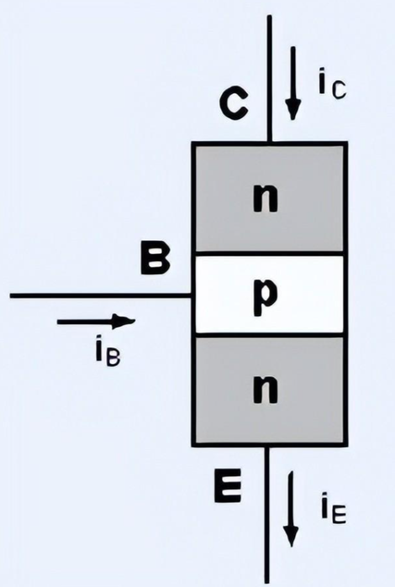
The 2N3904 is an NPN transistor used in general-purpose switching or low-power amplification applications.
Primarily designed for medium voltage, low power applications and operating at medium high speeds.
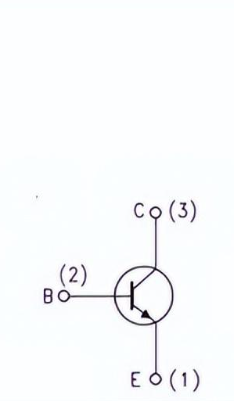
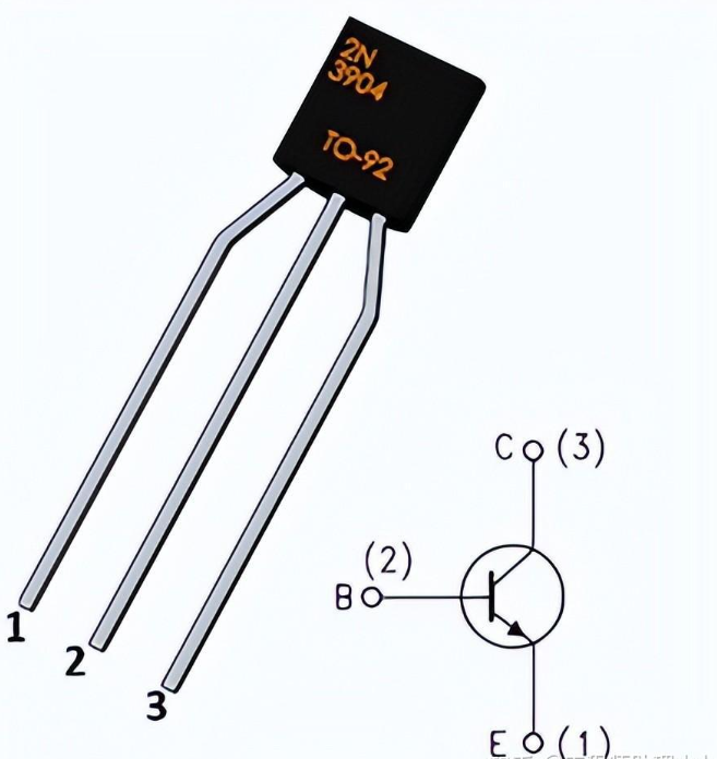
2--2N3904 Pin diagram and parameters
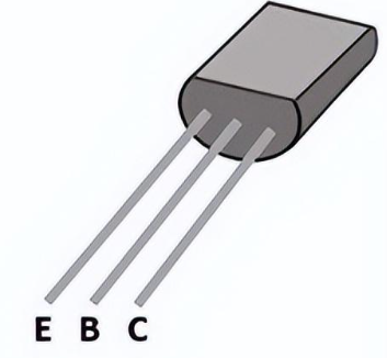
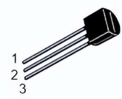
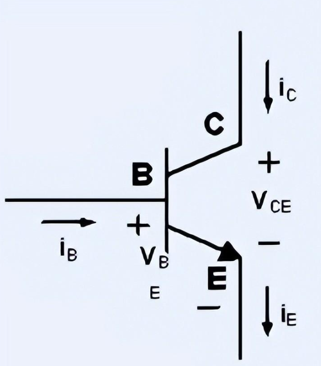
The 2N3904 transistor consists of three pins:
- Pin 1 (emitter) : Current will flow through this terminal.
- Pin 2 (base) : This pin controls the transistor bias.
- Pin 3 (collector) : Current supply to the entire terminal.
3--2N3904 triode parameters
- Collector current (Ic) (Max.) : 200mA
-
- Dc current gain or hFE (Max.) : 300
-
- Dc current gain or hFE (min) : 100@150mA, 10V
-
- Collector emitter voltage (Vce) : 40V
-
- Base to emitter voltage (Vbe) : 6V
-
- Collector-base voltage (Vcb) : 60V
-
- Vce saturation (maximum) under Ib and Ic conditions: 500mV@50mA, 500mA
-
- Power - Max: 800mW
-
- Frequency to conversion: 100MHz
-
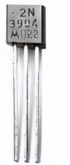
- Package/housing: TO-39-3, TO-205AD
- High voltage gain: The 2N3904 has a high voltage gain and is suitable for use in amplification circuits.
- Low noise: The transistor has a low noise figure, which is very useful in low-level signal amplification applications.
- High current gain: The 2N3904 has a high current gain, which is suitable for driving loads such as relays and lights.
- Fast switching speed: The transistor's fast switching speed makes it ideal for switching applications.
- Low cost: 2N3904 is cheap.

4--2N3904 How transistors work
In a 2N3904 transistor, most of the charge carriers are electrons, so they are always negatively charged.
The state of the transistor can be switched on from reverse bias to forward bias based on a small voltage at the base terminal (e.g. 0.7V).
- Base voltage (Vb) > emitter voltage (Ve).
- Collector voltage (Vc) > Base voltage (Vb).
If the base pin is connected to the GND terminal, both the emitter and collector terminals are reverse-biased or remain open.
Again, once the signal is fed to the base pin, it will be forward-biased.
The 2N3904 triode has a high gain value of 300, which determines its amplification capacity.
The maximum current supply at the collector terminal is 200mA, so loads consuming more than 200mA cannot be connected through this transistor.
Once a current source is supplied to the base terminal, the transistor can be biased. The IB current must be limited to 5mA.
When the 2N3904 NPN transistor is fully biased, it allows up to 200mA of current to flow through two specific terminals,
the emitter and the collector, in a specific phase called the saturation region. In addition,
the collector-emitter/collector-base terminals are capable of handling typical voltages of 40V and 60V respectively.
Once the base current is separated, the transistor will be turned off, so this stage is called the cutoff region, and the VBE may be around 600mV.
5--What triode can be used instead of 2N3904?
1. Equivalent transistor
BC636\BC547\BC549\BC639\2N2222 TO-18\2N2222 TO-92\2N2369\2N3906\2N3055\2SC5200 ...
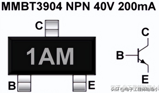
2. 2N3904 SMD
This article will not be repeated here for the time being
6--2N3904 uses
A step-by-step guide to using 2N3904 transistors as switches:
1) Understand pin arrangement
It is important to understand the pin configuration of the 2N3904 transistor.
- Vcontrol is the control signal voltage
- VBE is the base-emitter voltage drop (about 0.7V for silicon transistors)
- Connect the emitter of the transistor to the ground or a common reference point.
- Connect the collector to the positive supply voltage and load.
- Connect the base to the control signal via the base resistance.
- Ensure correct polarity when connecting load and power;
When the base current exceeds the threshold, the transistor enters the saturation region and conducts current between the collector and emitter, effectively "turning on" the load.
ensuring the function of transistors and other components.
2N3904 transistor as a switch practical case
the collector is powered, the LED is connected to the resistor (current limiting) at the emitter, and the other end is grounded.
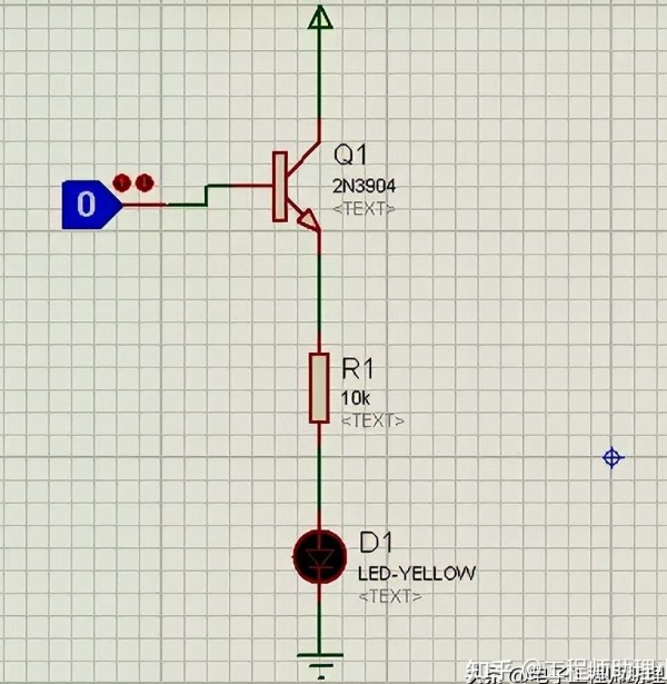
Since no voltage is applied to the base, the 2N3904 is in a reverse-biased state,
so the LED goes out. Now, when we apply 5V voltage to the base,
2N3904 gets a forward bias and now the LED lights up, as shown below:
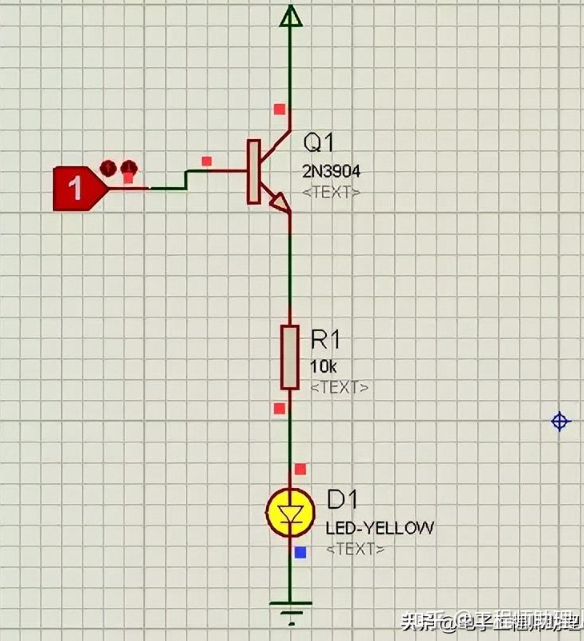
In the above simulation, a simple LED is controlled and a manual switch is used.
2, 2N3904 as an amplifier
Its versatile nature and availability make it suitable for a variety of applications where signal amplification is required.
When used as an amplifier, the 2N3904 operates in its active region, where a small input signal is amplified to produce a larger output signal.
1) Pin arrangement
Familiarize yourself with the pin configuration of the 2N3904 transistor, as above.
2) Bias transistor
A suitable DC bias is established for the transistor by applying a suitable voltage to the base-emitter junction.
Connect one capacitor in series with the input signal of the base terminal and the other capacitor in series with the output signal of the collector terminal.
the input impedance of the amplifier matches the source impedance,
and the output impedance of the amplifier matches the load impedance.
Adjust the bias network, such as the voltage divider resistance, to reach the desired operating point and optimize the amplifier's performance.
- Common emitter amplifier
- Common-collector amplifier
- Common-base amplifier
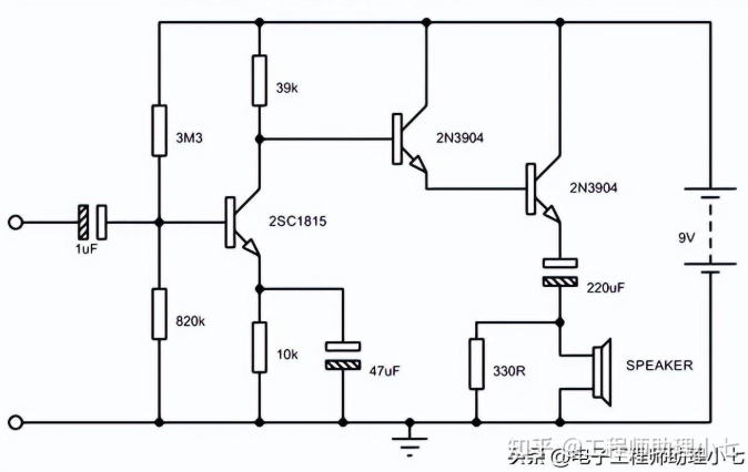
2N3904 as an amplifier example
In this simple amplifier circuit using transistor 2N3904, any input signal needs to pass through capacitor C1.
The input is the feed from the filter to the Q1 base after removing all signals except the sound signal.
Q1 is set to the common-emitter version of the amplifier circuit.
The voltage divider circuit of Q1 needs to connect R1 and R2. Q1 collector output signal is insufficient.
Therefore, this signal must now be increased again through Q2 and Q3.
The circuit includes the Darlington circuit of Q2 and Q3. Now, the signal has better gain, and from there is driven through the C3 to the SP1 speaker.
- amplifier
- Driver module (LED, motor or relay driver)
- Switch
- Voltage regulator
- convertor
- timer
- Frequency modulator
- PWM (Pulse Width Modulation)
- Signal processing circuit
- Audio circuit
- Power supply circuit
- comparator
The above is today's content, have the opportunity to share again, please give a lot of advice.
Blog Category
BlogsLatest Products

-
IP5002CX8/P135
NXP USA Inc.

-
ADAU7002ACBZ-RL
Analog Devices Inc.

-
PGA2320IDW
Texas Instruments

-
SRC4184IPAG
Texas Instruments

-
MUSES72320V-TE2
Nisshinbo Micro Devices Inc.

-
PCM2706CPJT
Texas Instruments

-
ZL38040LDG1
Microchip Technology
-
PGA2310UA/1K
Texas Instruments
Get Started Instantly!
Get the Latest News
